Basic Comparison
Comparison of a GaAs and SiGe Process
Active and passive components can be integrated together on a single die (or "chip") of GaAs in much the same way as their more conventional silicon counterparts. However GaAs has certain advantages over Si,particularly for higher frequency applications:
Higher electron mobility means devices with higher upper operating frequencies can be fabricated.
The semi-insulating nature of undoped GaAs means higher Q passive components can be produced and higher device to device isolation is more readily achieved.
Most GaAs processes offer low loss through substrate” via-holes" connecting the front side of the wafer to the back. This provides a means of realizing low inductance RF ground connections.
One of the advantages of integrated realizations is that large numbers of a given circuit can be fabricated at one time on a single wafer.
Due to substrate doping, SiGe based circuits contain more “lossy” passive components, such as spiral inductors and capacitors. And because components on the integrated circuit will capacitively couple to the “lossy” substrate, circuit performance will degrade. GaAs based circuits on the other hand do not have this problem because the substrate is not doped and it acts as an excellent insulator at millimeter wave frequencies.
Also, the metallization schemes used for most SiGe circuits are aluminum based, whereas GaAs circuits almost exclusively use gold based metallization. Aluminum based metallization have higher resistivity than gold, thus leading to lower Q passive components. This means that the Q-factor of spiral inductors on GaAs will be about much higher as those on Silicon.
From an end-product point of view, this often means more “off-chip” components will be required for a SiGe circuit than for a GaAs circuit. This in turn results in more board area consumed by the SiGe product and higher total cost, both for the extra off-chip components themselves, and for the cost of placing the components on the manufacturer’s board.
Comparison of GaAs and SiGe Based Technology
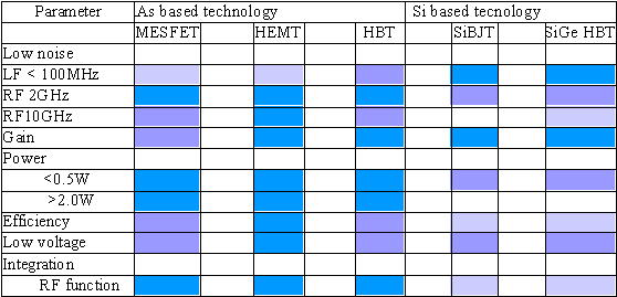
Silicon Germanium Heterojunction Bipolar Transistors (HBTs) have higher minimum noise figures than equivalent Gallium Arsenide MESFETs or PHEMTs .This is due to shot noise from the base-to-emitter diode junction of a SiGe HBT, which is not present in GaAs based MESFETs or PHEMTs.
Under normal operation, current flows through the base-to-emitter in SiGe HBTs and is proportional to the collector current by 1/Beta of the transistor (typically between 100-300). This means that the base-to-emitter diode junction is turned on and will generate more noise than a GaAs FET where the gate-to-source voltage is well below the diode turn-on voltage (under normal bias conditions for low noise operation).
Also, the minimum noise figures of SiGe HBTs increase rapidly as a function of collector current, whereas GaAs MESFETs or PHEMTs remain low over a wide range of drain current. This allows for a better trade off between linearity (output 3rd order intercept point, OIP3), noise figure, and bias current in GaAs FETs than SiGe HBTs.
For SiGe HBTs, the best linearity figure of merit LFOM is achieved at currents ranging from 10 mA to 15 mA whereas peak LFOM in GaAs FETs is found at currents ranging from 2 mA to 6 mA. These are typical numbers assuming a +3 V collector/drain supply and equivalent device sizes.
 For wireless power amplifier (PA) applications, the ideal device should have very good linearity, be efficient at low voltage operation and need only simple biasing control. In addition, the technology must have a high enough breakdown voltage to be able to withstand high VSWRs and handle the heat dissipation. Generally, the heat dissipation precludes adding other RF functions to the power amplifier. Therefore, the level of integration for power amplifiers is moderate at most. GaAs/AlGaAs HBT offers these attributes and is optimal technology when compared to MESFETs and SiGe HBT. For wireless power amplifier (PA) applications, the ideal device should have very good linearity, be efficient at low voltage operation and need only simple biasing control. In addition, the technology must have a high enough breakdown voltage to be able to withstand high VSWRs and handle the heat dissipation. Generally, the heat dissipation precludes adding other RF functions to the power amplifier. Therefore, the level of integration for power amplifiers is moderate at most. GaAs/AlGaAs HBT offers these attributes and is optimal technology when compared to MESFETs and SiGe HBT.
While SiGe HBT does offer excellent linearity and noise figure for such applications as front end LNAs, it does lack the high voltage-handling attribute required for PA applications.
General strength of the GaAs technologies is to integrate RF functions into the MMICs in lumped elements, stripline or coplanar design. This makes them the primary source for integrated multifunction RF devices in the microwave area.
The Si technologies have the advantage of the integration of analog bipolar functions with the VLSI CMOS world. This gives the opportunity to integrate D/A converters and mixed signal applications.
Comparative analysis on GaAs and Si based technology. Download in PDF
|